

赫狄通納米
主營(yíng)產(chǎn)品: 納米材料
銅基底CVD單層石墨烯(2.5cm*2.5cm)
價(jià)格
訂貨量(件)
¥2400.00
≥1
店鋪主推品 熱銷潛力款
䝒䝐䝔䝒䝘䝗䝕䝘䝕䝐䝑
在線客服
生產(chǎn)廠商:Graphene Platform (Japan)
產(chǎn)品信息
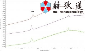
§ Graphene quality and thickness are confirmed by Raman spectroscopy.
§ Multi-point Raman data are provided with every sample.
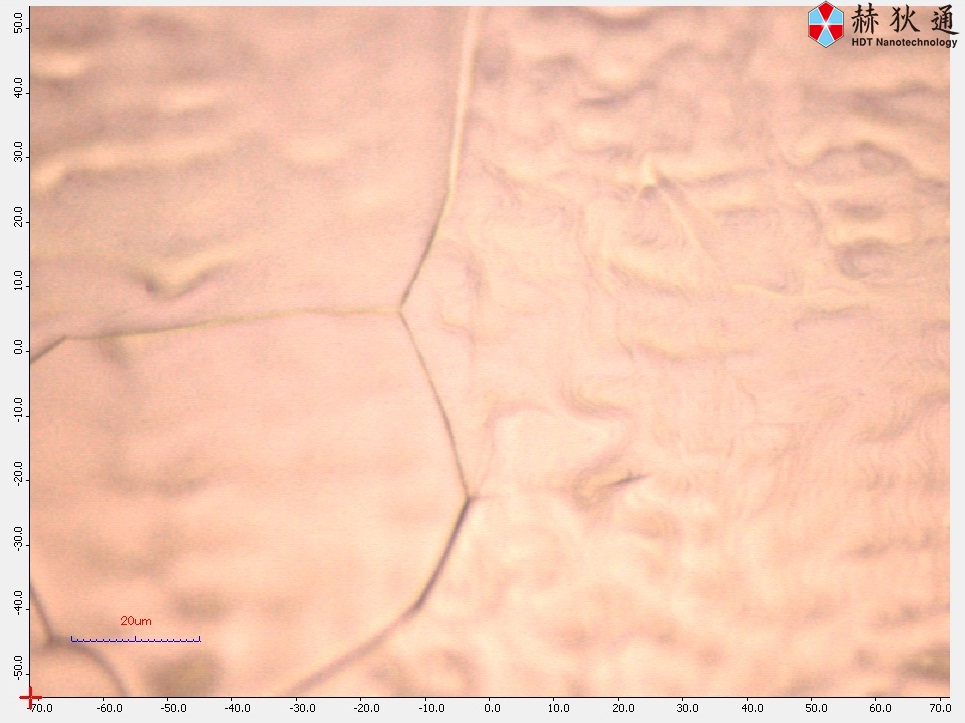
§ Graphene layer is continuous with few small multilayer islands and overall coverage exceeding 95%.
§ Sheet resistance is < 1,000 ohm per square.
§ Optical transmission is > 95%.
§ Copper foil thickness: 35 micron.
§ All samples are manufactured in our lab in Japan.


1. Raman spectroscopy is used to check the presence of a D peak in graphene samples. If a D peak is present, then this can indicate defects in the sample, such as cracks or flaking.
2. The ratio of the heights of the 2D peak and the G peak indicate the number of graphene layers.
2D>G : Single-layer
2D=G : Double layer
2D<G : more than triple layer
3. 3 measurements for every sample are taken and presented on the same graph.
采購(gòu)數(shù)量不能為空
聯(lián)系信息不能為空

驗(yàn)證碼不正確