找商網(wǎng)手機端:m.zhaosw.com


赫狄通納米
主營產(chǎn)品: 納米材料


基于285nm氧化層硅基底的CVD石墨烯氮化硼異質(zhì)結(jié)薄膜
價格
訂貨量(件)
¥4000.00
≥1
店鋪主推品 熱銷潛力款
㜉㜆㜃㜉㜌㜋㜊㜌㜊㜆㜄
在線客服
生產(chǎn)廠商:Graphene Supermarket
產(chǎn)品信息
CVD Graphene/CVD Hexagonal Boron Nitride heterostructure on SiO2/Si wafer
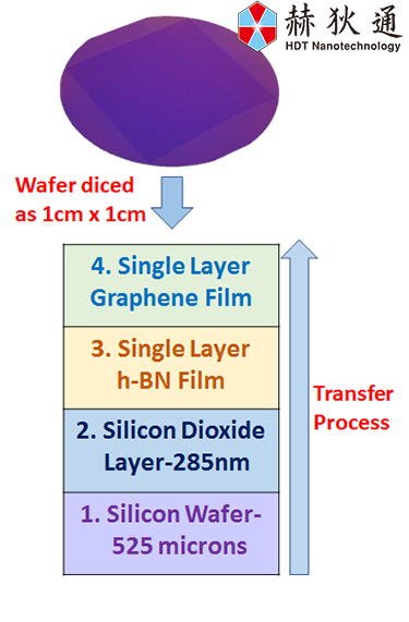
Single Layer Graphene Film on Single Layer h-BN Film transferred onto 285 nm (p-doped) SiO2/Si wafer
Size: 1cmx1cm; 4 pack
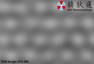
The thickness and quality of each film is controlled by Raman Spectroscopy
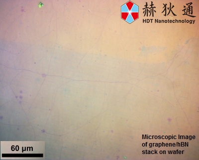
The coverage of this product is about 98%
The films are continuous, with minor holes and organic residues
High Crystalline Quality
The graphene film is premodominantly single layer (more than 95%) with occasional small multilayer islands (less than 5% bi-layers)
Sheet Resistance: 430-800 Ω/square
Oxide Thickness: 285 nm
Color: Violet
Wafer thickness: 525 micron
Resistivity: 0.001-0.005 ohm-cm
Type/Dopant: P/Boron
Orientation: <100>
Front Surface: Polished
Back Surface: Etched
Graphene/hBN interfaces are used where the graphene needs to be precisely gated, for increased mobility, and for reduced scattering.
h-BN is appealing as a substrate for graphene-based electronics because its surface is atomically smooth, it is free of dangling bonds, and has an analogous structure to graphene.
Using our h-BN on SiO2/Si wafers in conjuction with graphene will encourage you to explore graphene heterostructures for transistor applications

周經(jīng)理
![]() 㜉㜆㜃㜉㜌㜋㜊㜌㜊㜆㜄
㜉㜆㜃㜉㜌㜋㜊㜌㜊㜆㜄

掃碼查看
手機掃碼 快速查看
采購數(shù)量不能為空
聯(lián)系信息不能為空
驗證碼不正確