

赫狄通納米
主營產品: 納米材料
基于285nm氧化層硅基底的CVD單層氮化硼薄膜(1*1cm-4片裝)
價格
訂貨量(件)
¥3650.00
≥1
店鋪主推品 熱銷潛力款
钳钶钴钳钸钵钻钸钻钶钺
在線客服
生產廠商:Graphene Supermarket
產品信息
97% coverage with minor holes and organic residues
High Crystalline Quality
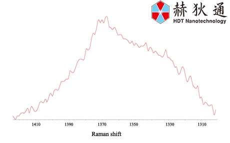
The Raman spectrum should peak at ~1369cm-1
The h-BN film is grown via CVD onto copper foil, then transferred to the SiO2/Si substrate
BN on SiO2/Si wafers are ideal for creating graphene/BN interfaces, allowing the graphene to be precisely gated, increasing mobility, and reducing scattering. h-BN is appealing as a substrate for graphene-based electronics because its surface is atomically smooth, it is free of dangling bonds, and has an analogous structure to graphene. Using our h-BN on SiO2/Si wafers in conjunction with graphene, we encourage you to explore graphene heterostructures for transistor applications.

The Raman spectrum of hBN monolayer
采購數量不能為空
聯系信息不能為空

驗證碼不正確